CREATE : PROTOTYPING : Fabricating PCBs
Once you've prototyped and tested your Scamp project, consider making your design permanent by creating your own PCB. It's a lot of fun, it can be very rewarding, and you can even sell your boards to others.
In this page, I will show you the process of submitting a PCB design for fabrication.
In this page, I will show you the process of submitting a PCB design for fabrication.
Typically, you start by creating a customer account with the manufacturer. Fill out your delivery address, contact details and any other information relevant to you. You will be assigned to a representative, who is your contact person at the company. Any questions you have, this is the person who will help you. You will find the customer service is generally very good.
Next, check out their page on production capabilities (this example is PCBWay) to make sure your design can be manufactured. It's worth revisiting this regularly as capabilities evolve and improve over time. I also check it over before choosing components for a design. Semiconductor manufacturers push toward ever smaller parts, and some parts with ultra small pin spacings can be problematic to have assembled into a design. You can save yourself a lot of redesign effort and cost by choosing parts early in the design process that make manufacturing easier.
Generating Files for PCB Fabrication
Once you've finished your PCB design, thoroughly check it over. Make sure there are adequate clearances between tracks, pads and other objects, check hole sizes are correct for any through-hole components to be mounted. Also consider mechanical clearances of components. If two bulky components are close to each other, they may mechanically interfere with each other when assembled. (Doing physical outlines of components in a mechanical layer of your PCB editor helps here. If your PCB editor does 3D rendering, that's also useful for checking mechanical clearances.)
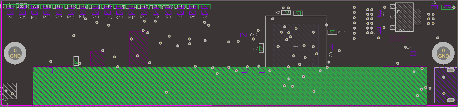
Mechanical outlines on the Scamp3
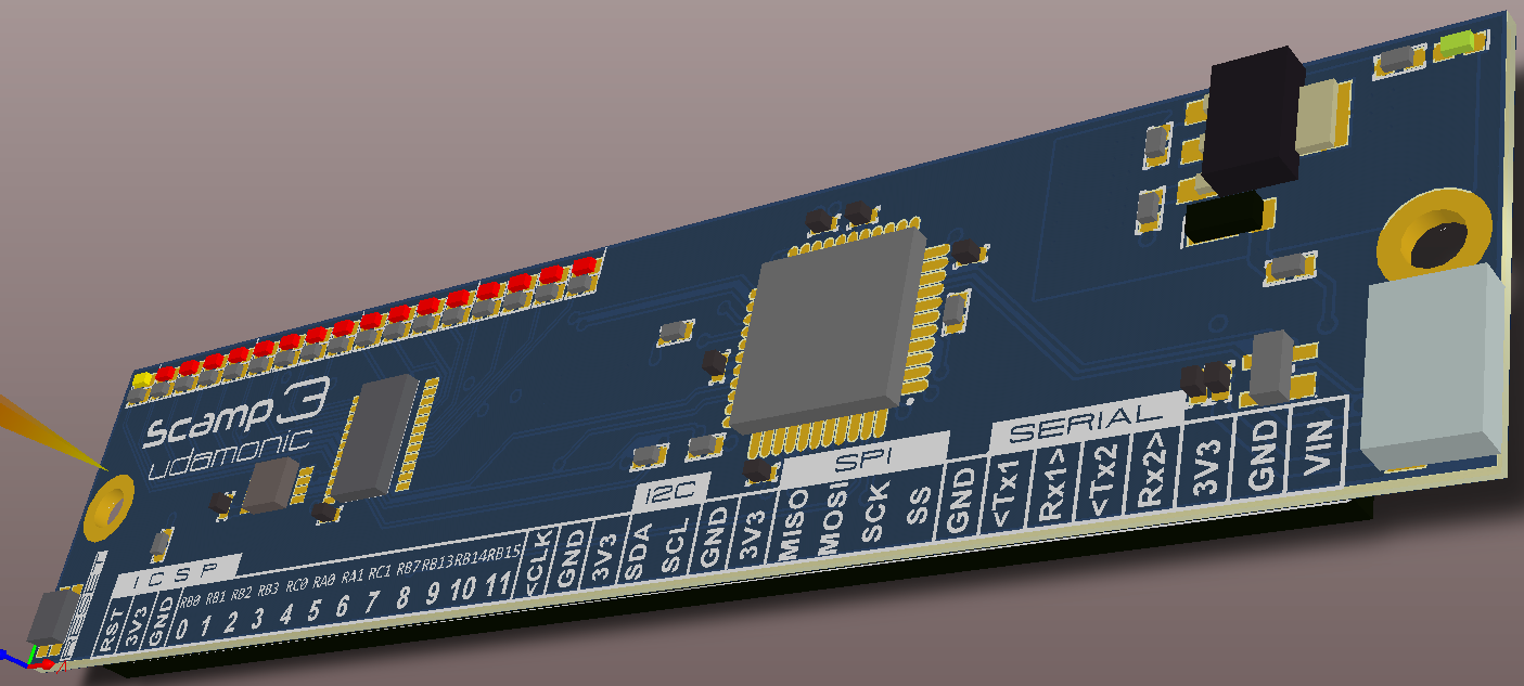
3D render of a Scamp3
To submit your design for manufacture, you will need to generate Gerber files and an NC Drill file. There will be a Gerber file for each layer you've used. These are ASCII vector files originally used to drive large photoplotters, but have now become the defacto standard for PCB fabrication. NC Drill files are also ACII format, and they drive the drill machines that create your holes. All PCB design software can generate Gerbers and NC Drill files, and all PCB manufacturers accept them. So although you may feel unfamiliar with them, just know that they are the industry standard.
|
When generating your Gerber files, make sure each layer you have used is selected.
|
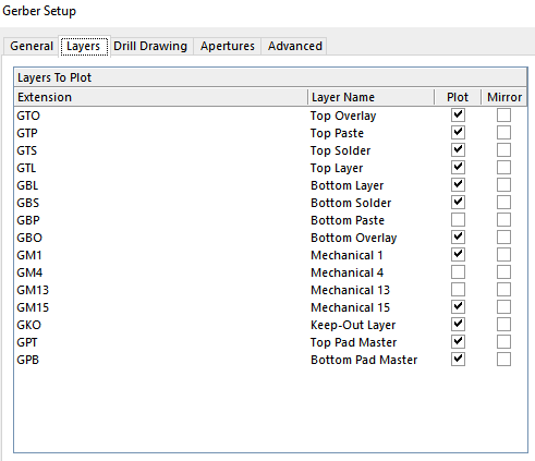
Gerber generation in Altium
|
Get yourself an application that can view Gerber files, and check over each layer. Sometimes you can spot design errors at this step that weren't obvious in the PCB editor. I use Cuprum (MacOS) for this.
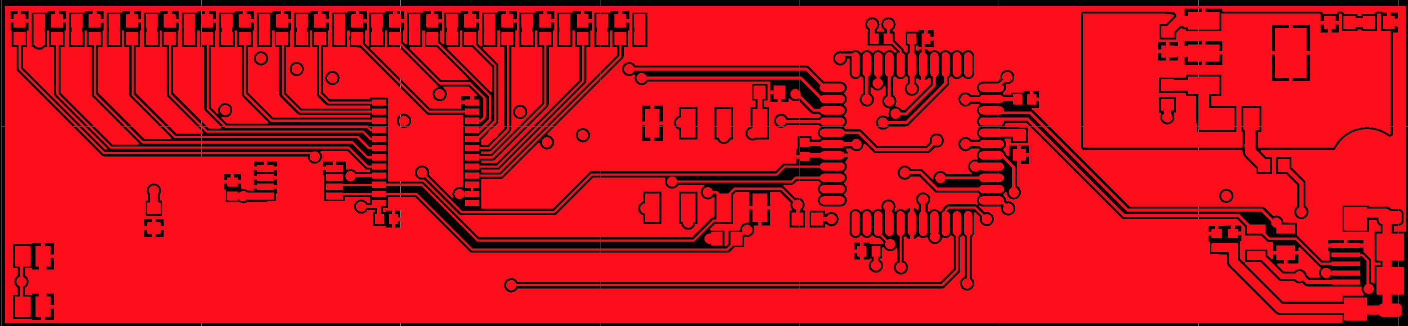
Gerber for Scamp3 Top Layer viewed in Cuprum
Put your Gerbers and NC Drill file into a single folder and ZIP it. Name the ZIP file appropriately for your project. The ZIP file is what you upload to the PCB manufacturer.
Submitting Your Design
|
The process starts on PCB manufacturer's front page, by filling out the "Instant Quote" panel. This will take you to a more detailed quote page.
|
|
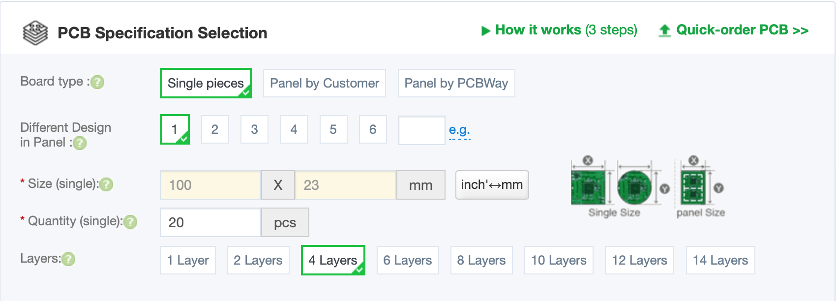
"Board type" indicates whether you want individual boards, or boards left unrouted in a panel. (All PCBs are panelized for manufacture, and if required for further post-manufacturing, they can be left in the panel.) Unless you have special requirements for a panel, just select "Single pieces".
You can have more than one board design in a panel. For most PCB runs. select "1" for a single design.
Specify the size of the individual PCB and the quantity required. The more PCBs you have made, the cheaper it gets. Play with quantity value and see how it affects the cost. For example, you might find you can get 200 PCBs for a similar cost to getting 20 made. Experiment to see what works best for your board and your situation.
Select the number of layers needed for your design.
Next, specify the parameters for this PCB build.
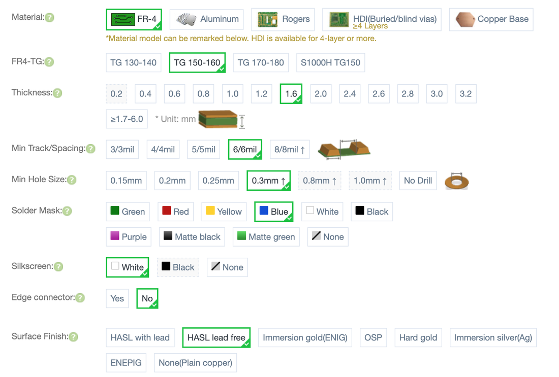
For most PCBs, FR-4 with 1.6 mm thickness is sufficient. Select this unless your design has special requirements. The default minimum spacing is 6 mil (6 thousandths of an inch). This is the minimum track spacing you've used on your PCB. The hole size is the minimum used in your design - typically this will be your via hole size since vias tend to be the smallest objects in a design.
Choose your solder mask color. This is the overall color of your PCB. Green is cheapest. The other colors can look more interesting. Your PCBs will be part of a process along with designs from lots of other customers. Commonly chosen parameters are cheaper. Unusual choice combinations can really add to the cost of manufacture, so choose carefully.
The Silkscreen color is your overlay layer. These are the painted labels applied to your PCB.
The Surface Finish refers to the plating on exposed pads. This is what your solder will bond with. "HASL" means "Hot Air Solder Levelling" and is the most common finish. Most countries require lead-free products, so select "HASL lead free" for your surface finish.
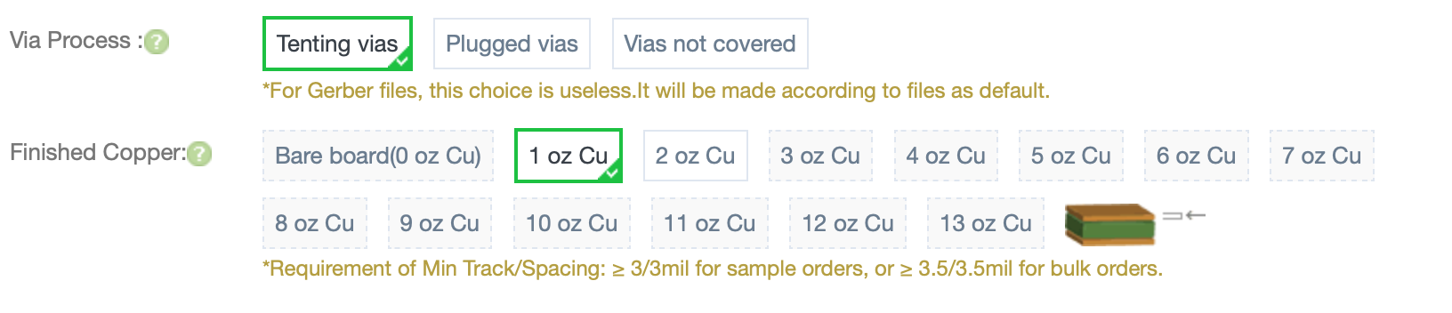
The via process is controlled by the Gerbers, so ignore this. (It's possible to submit designs in other formats, in which case the via process needs to be specified.)
Choose your copper thickness, 1 oz is typical. And you're done. Click "Save to Cart" on the right side of the page. You will be taken to a page to upload your ZIPped Gerbers and NC Drill file.
Choose your copper thickness, 1 oz is typical. And you're done. Click "Save to Cart" on the right side of the page. You will be taken to a page to upload your ZIPped Gerbers and NC Drill file.
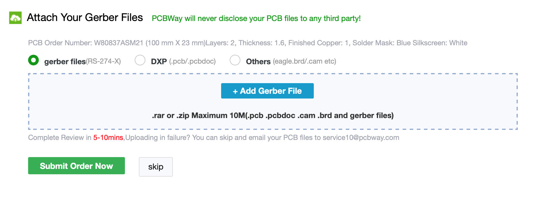
Submit your order. It will be reviewed by a production engineer at the PCB manufacturer relatively quickly, and once passed you will be asked for payment. Once the build is underway, you can track the production process through your account. Within a few days, your PCBs will be on their way to you.
|
|
|
|