DataFlash
|

|
|
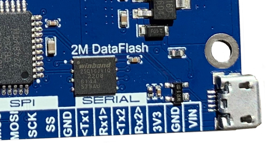
The Scamp3e has a W25Q16JV 2Mbyte dataflash with a SPI interface, for persistent storage of data. The W25Q16JV array is organized into 8,192 programmable pages of 256-bytes each. Pages can be erased in groups of 16 sectors (4K each), groups of 128 blocks (32KB block erase), groups of 256 blocks (64K block erase) or the entire chip (chip erase). The W25Q16JV has 512 erasable sectors and 32 erasable blocks respectively. The small 4KB sectors allow for greater flexibility in applications that require data and parameter storage.
|
|
Memory Map
The W25Q16JV has a total capacity of 2 MB (2,097,152 bytes), divided internally as follows:
Here’s how the address space is arranged conceptually:
- 8,192 pages × 256 bytes = 2,097,152 bytes (2 MB)
- 512 sectors × 4 KB = 2,097,152 bytes (2 MB)
- 32 blocks of 64 KB = 2,097,152 bytes (2 MB)
Here’s how the address space is arranged conceptually:
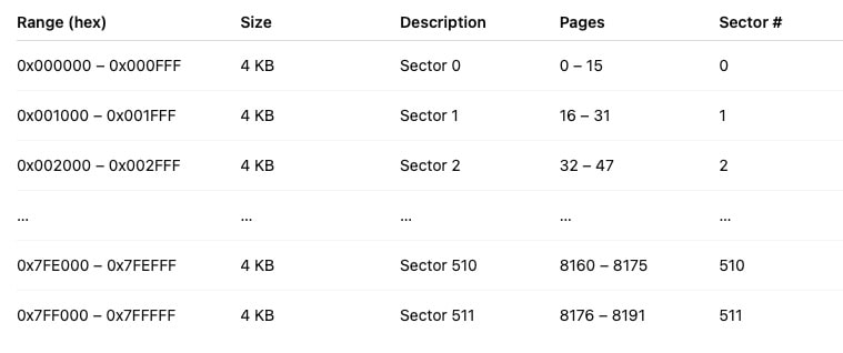
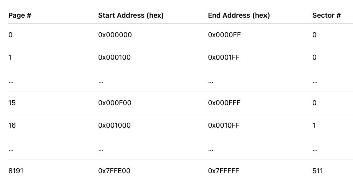
Each sector consists of 16 pages, each 256 bytes long. Each page starts at a 256-byte boundary, so page n starts at address n × 0x100 (hex).
To show this relationship more explicitly:
To show this relationship more explicitly:
Writing Data to the Dataflash
The most efficient way to use the dataflash is to write an entire page of 256 bytes at a time. Writing smaller blocks of data repeatedly can cause excessive wear on the chip and is best avoided. The dataflash consists of 8,192 ($2000) individually programmable pages.
First, we need to create a buffer in memory to hold the data to be written. We allot 256 bytes for the buffer.
First, we need to create a buffer in memory to hold the data to be written. We allot 256 bytes for the buffer.
create mybuff #256 allot
Next you fill your buffer with data. This might be sensor data, or comms traffic, or whatever. But for this example, we'll create a word to fill the buffer with a sequence of numbers:
: myfill
#256 for
i mybuff i + c!
next
;
myfill
You can check the buffer in memory using the word dump:
hex
mybuff #256 dump
1144 :00 01 02 03 04 05 06 07 08 09 0a 0b 0c 0d 0e 0f ................

1154 :10 11 12 13 14 15 16 17 18 19 1a 1b 1c 1d 1e 1f ................

1164 :20 21 22 23 24 25 26 27 28 29 2a 2b 2c 2d 2e 2f  !"#$%&'()*+,-./

1174 :30 31 32 33 34 35 36 37 38 39 3a 3b 3c 3d 3e 3f 0123456789:;<=>?

1184 :40 41 42 43 44 45 46 47 48 49 4a 4b 4c 4d 4e 4f @ABCDEFGHIJKLMNO

1194 :50 51 52 53 54 55 56 57 58 59 5a 5b 5c 5d 5e 5f PQRSTUVWXYZ[\]^_

11a4 :60 61 62 63 64 65 66 67 68 69 6a 6b 6c 6d 6e 6f `abcdefghijklmno

11b4 :70 71 72 73 74 75 76 77 78 79 7a 7b 7c 7d 7e 7f pqrstuvwxyz{|}~.

11c4 :80 81 82 83 84 85 86 87 88 89 8a 8b 8c 8d 8e 8f ................

11d4 :90 91 92 93 94 95 96 97 98 99 9a 9b 9c 9d 9e 9f ................

11e4 :a0 a1 a2 a3 a4 a5 a6 a7 a8 a9 aa ab ac ad ae af ................

11f4 :b0 b1 b2 b3 b4 b5 b6 b7 b8 b9 ba bb bc bd be bf ................

1204 :c0 c1 c2 c3 c4 c5 c6 c7 c8 c9 ca cb cc cd ce cf ................

1214 :d0 d1 d2 d3 d4 d5 d6 d7 d8 d9 da db dc dd de df ................

1224 :e0 e1 e2 e3 e4 e5 e6 e7 e8 e9 ea eb ec ed ee ef ................

1234 :f0 f1 f2 f3 f4 f5 f6 f7 f8 f9 fa fb fc fd fe ff ................ ok
We can then place the address of the buffer on the stack, followed by the page number we want to write, and then use page! to write the data into the dataflash:
mybuff 3 page!
|
|
Note: once a page is written to, it can't be rewritten with new data until it is first erased. See the section below on erasing sectors and blocks within the dataflash.
|
|
Reading a single Value from the DataFlash
The word df@ will read a 16-bit value from a location within the dataflash, and place the value on the stack. For example, to read page 3, location 10:
3 10 df@
The word dfc@ will read an 8-bit value from a location within the dataflash, and place the value on the stack. For example, to read the byte at page 3, location 10:
3 10 dfc@
Reading an Entire Page from Dataflash to RAM
The word page@ will read a page from the dataflash to a buffer in memory. But to prove that it works, first lets fill our buffer in memory with zeroes:
mybuff $100 0 fill
mybuff $100 dump
Now, to read dataflash page 3 to mybuff in memory, and examine the contents:
mybuff 3 page@
mybuff $100 dump
Dumping a Flash Page to the Console
The following word definition will read 256 bytes (128 16-bit integers) from a dataflash page and output it to the console:
\ dumps a flash page to the console
\ 128 16-bit values, use in hex base
: pagedump ( page -- )
cr
0 \ index, first address in page
#16 for
#8 for
over over \ copy page # and page index
df@ #4 u.r \ read data and print formatted
2+ \ inc address
next cr
next
2drop
;
To dump dataflash page 3 to the console:
hex
3 pagedump
Erasing Sectors and 64K Blocks
Each page can be individually programmed after being erased. Data can only be programmed from a logical ‘1’ to ‘0’ - erasure is required to reset bits back to ‘1’.
Erase operations can be performed at several granularities:
To erase a sector or block, first the dataflash must be unlocked using dfUnlock, then write must be enabled with dfWE. Finally the chip can be erased with either SectorErase or BlockErase. Note that a sector or block erase can take several seconds to complete. The Scamp3e status LED will light during the erase cycle.
To erase sector 3:
Erase operations can be performed at several granularities:
- Sector erase (4 KB) – the smallest erase unit, comprising 16 pages.
- 32 KB block erase – comprising 128 pages.
- 64 KB block erase – comprising 256 pages.
- Chip erase – erases the entire 2 MB array.
To erase a sector or block, first the dataflash must be unlocked using dfUnlock, then write must be enabled with dfWE. Finally the chip can be erased with either SectorErase or BlockErase. Note that a sector or block erase can take several seconds to complete. The Scamp3e status LED will light during the erase cycle.
To erase sector 3:
dfUnlock dfWE 3 SectorErase
To erase (64K) block 2:
dfUnlock dfWE 2 BlockErase
Erasing the whole Dataflash
To erase the entire chip, first the dataflash must be unlocked using dfUnlock, then write must be enabled with dfWE. Finally the chip can be erased with FlashErase. Note that a full chip erase can take up to 25 seconds to complete. The Scamp3e status LED will light during the erase cycle.
dfUnlock dfWE FlashErase
Manually Accessing the DataFlash
The dataflash has many commands available. Refer to the datasheet for a complete list. The word dfSel will select the dataflash's chip select prior to a SPI transfer. The word dfDesel will deselect the chip select at the completion of a SPI transfer. For an example of manually sending a dataflash command, see FlashID in the next section.
The word dfWait can be used to check the busy status of the dataflash during long operations, and will light the Scamp3e status LED until the operation is complete. dfWait is used within SectorErase, BlockErase and FlashErase.
dfUnlock will unlock the dataflash for erasing. dfLock can used to lock the dataflash.
dfWE will enable the dataflash for writing. It is called automatically by page! but must be manually called when erasing sectors, blocks or the entire chip.
dfReset will send a soft reset command to the dataflash. In general use, this is not normally required.
FlashID
The following word definition will read the ID parameters from the dataflash and output these to the console. (Use in hex mode.) Refer to the dataflash datasheet for more info.
: FlashID
8 spisize
dfSel
\ read ID command
$4b spix drop
\ send 32 dummy clock cycles
#16 spisize
0 spix drop
0 spix drop
\ read back four 16 bit codes and display them
0 spix u. 0 spix u. 0 spix u. 0 spix u.
dfDesel
;
Learn : Interfacing : DataFlash